PCBs, or printed circuit boards, are crucial parts of contemporary electronics. This article explores the full form of PCB, its history, types, applications, and the manufacturing process.
What is PCB?
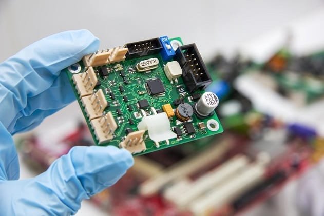
PCB stands for Printed Circuit Board. It is a board used in electronics to connect and support electronic components. These boards are found in almost every electronic device, from smartphones to computers to industrial machines. Baji999 login offers secure access to online gaming, featuring diverse casino games and sports betting. Enjoy a user-friendly experience with protected data, delivering thrilling entertainment for all users.
History of PCBs
The concept of PCBs dates back to the early 20th century. you can make money on Bet Winner APK.
- 1903: German inventor Albert Hanson filed a patent for flat foil conductors laminated to an insulating board.
- 1943: Paul Eisler, an Austrian engineer, developed the first true PCB for use in radios.
- 1950s: The mass production of PCBs began, revolutionizing electronics manufacturing.
Types of PCBs
There are several types of PCBs, each serving different purposes:
Single-Sided PCBs
- Features: Conductive copper layer on one side of the board.
- Applications: Simple electronics, calculators, and power supplies.
Double-Sided PCBs
- Features: Conductive layers on both sides with vias connecting the layers.
- Applications: Amplifiers, automotive dashboards, and power monitoring systems.
Multi-Layer PCBs
- Features: Multiple layers of conductive material separated by insulating layers.
- Applications: Complex devices like computers, medical equipment, and aerospace electronics.
Flexible PCBs
- Features: Made of flexible materials that allow bending and flexing.
- Applications: Wearable devices, flexible solar cells, and medical devices.
Rigid-Flex PCBs
- Features: Combination of rigid and flexible substrates.
- Applications: Smartphones, cameras, and military applications.
Applications of PCBs
PCBs are ubiquitous in various industries, including:
- Consumer Electronics: Smartphones, tablets, and home appliances.
- Automotive: Engine control systems, infotainment systems, and safety devices.
- Medical: Diagnostic equipment, imaging devices, and patient monitoring systems.
- Industrial: Machinery control systems, power converters, and robotics.
- Aerospace: Avionics, communication systems, and navigation equipment.
PCB Manufacturing Process
Creating a PCB involves several steps:
Design
- Software Tools: Engineers use CAD software to design the PCB layout.
- Schematic Diagrams: These diagrams represent the electronic circuits on the PCB.
Printing the PCB
- Photomask Creation: A photomask is created from the design.
- Substrate Preparation: The PCB substrate is cleaned and prepared.
- Layer Imaging: Layers of the PCB are imaged using UV light through the photomask.
Etching
- Removing Excess Copper: Chemical solutions etch away unwanted copper, leaving only the desired circuit patterns.
Drilling
- Creating Holes: Precision drills create holes for component leads and vias.
Plating
- Adding Conductive Layers: Holes and surfaces are plated with copper.
Solder Mask Application
- Protective Coating: A solder mask is applied to protect the copper circuits and prevent short circuits.
Silkscreen Printing
- Component Labels: Identifying labels and markings are printed on the PCB.
Assembly
- Placing Components: Electronic components are placed on the PCB.
- Soldering: Components are soldered to the board, ensuring electrical connections.
Conclusion
Modern electronics cannot function without PCBs, which are essential to the operation of many everyday items. Understanding their types, applications, and manufacturing process highlights their importance in the technological world.
For further inquiries about PCB Full Form and their applications, consider exploring additional resources or consulting with electronics experts.